RFX400 daughterboard modification
Contents |
Introduction
The RFX400 can work from 400Mhz to 500 Mhz with a total power up to 200 mW. To use it for the band III on the channels 10,11,12 we need to make some modification.
The conversion is done with a quadrature modulator (AD8345) taking the two DAC's USRP TX port signal and a carrier from a built in programmable local oscillator (PLL using one ADF4360). The card include also for the TX path 2 stages of amplification before a low pass filter. The bandwidth of the last stage will not go under 300 Mhz (According to the spec. of the RF3315 rated for 0.3 to 3 Ghz).
Changing the VCO range
If you try to use this card under 400 Mhz you need at least to change the inductances value of the PLL VCO. (It won't lock outside the original band otherwise). According to the chip data-sheet the correct value to operate on the VHF band III is around 22 nH.
Inductors values
Here's a table showing the range of operation depending on the inductance value (derived from ADF4360 formula):
| L | VCO frequency | Operation bandwidth | Min ouput frequency | Max output frequency |
|---|---|---|---|---|
| 18nH | 464'936'224 | 61'991'497 | 201'472'364 | 263'463'861 |
| 22nH | 422'383'112 | 56'317'748 | 183'032'682 | 239'350'430 |
| 27nH | 382'668'034 | 51'022'405 | 165'822'815 | 216'845'219 |
Changing inductors
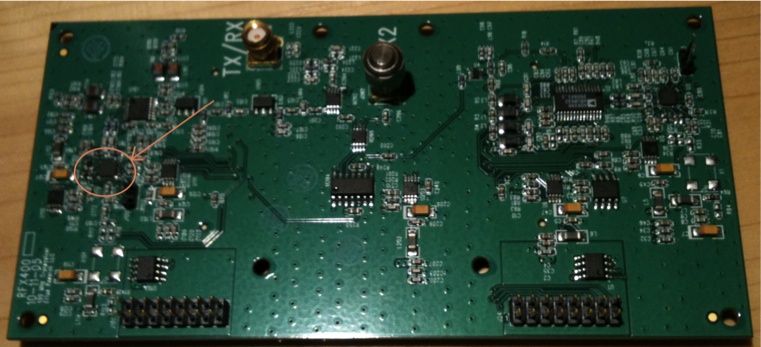
Locate the TX PLL:
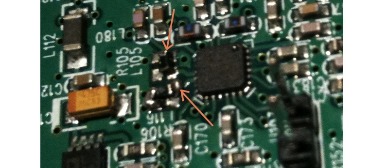
Then replace L105 and L115 inductances (in // with R105 and R106)
(Note: Since the RFX400 use the same PLL design beetween RX and TX side, this could be done at the RX path, if you want to receive signal on the same band, just replace L31 & L32 as done at the TX side)
We had no problem after this modification to lock beetween 200 to 235 Mhz. (Note: When having RFX400 and BasicTx installed simultaneously inside the USRP the software will adress by default the BasicTX !)
Whithout changing the amplifier (remember, we are bellow 300 Mhz the lower limit of the last stage) we still have an average of 5 mW at the output.
Ouput spectrum
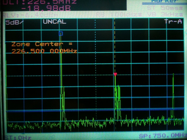
Here's the output spectrum of the RFX400 after VCO modification:
We see that working below the original board band will require to change the value of the on-board lowpass filter in order to kill the upper harmonics (that are now under the cutoff frequency of the filter, around 500MHz). The signal with the blue square is the wanted signal while the signal with the red marker is his first harmonic (in the original RFX400 band).The ratio beetween the in-band signal and the first harmonic is also degraded by the fact that we didn't change the final amplifier stage, further improvments needs to be done...
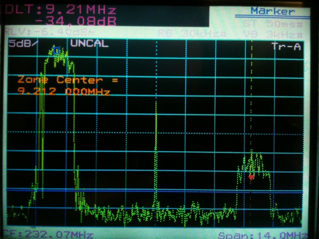
A closer look to the inband signal:
The LO leakage (center carrier on the picture) remain to high and require a strong attenuation before putting on the air this signal.
As the signal center frequency (modulated groupe of carriers from the OFDM signal) coming from the DAC's is quite low (4,7 Mhz) it keep the beat too close of the LO, making this hard to filter it efficiently without disturbing the linearity on the OFDM channel.
We also see that the upper beat signal (LO + 4,7 Mhz) is visible at 30 dB under the lower beat (LO – 4,7 Mhz = wanted signal). We should have a balance problem between the two inputs of the quadrature modulator (DC offset ? Averaging in the FPGA when computing the complex signal ? Resistors precision after the DAC's ?) This need to be investigated ...
As different elements of this spectrum are not so easy to filter (very close in frequency) it might be wise to change the center frequency leaving the DAC's (limited by the sampling rate) to make a wider space and use a higher LO frequency. This to put a fixed mask filter after the DAC's, then low pass filters after the quadrature modulator to kill the LO, the upper beat signal (if we cannot balance perfectly the input source at the modulator) and higher harmonics. Then we will replace the final stage of the RFX400 board by a monolytic amplifier having a lower 'start frequency'. TBC...


