Difference between revisions of "Example of RF amplifier for DAB"
| (78 intermediate revisions by 2 users not shown) | |||
| Line 1: | Line 1: | ||
[[Image:Amp1.jpg]] | [[Image:Amp1.jpg]] | ||
| − | + | Interesting ? Yes but... before thinking to use this kind of gizmo after the USRP, the RF signal need some manipulations, avoiding any disturbance on the radio spectrum. | |
| + | |||
| + | *Update 24/2/2010: Check the new [[WBX daughterboard]] test, a big improvement for a clean spectrum ! | ||
| + | |||
<big><b> NEVER CONNECT TO AN ANTENNA WITHOUT A LICENSE ! </b></big> | <big><b> NEVER CONNECT TO AN ANTENNA WITHOUT A LICENSE ! </b></big> | ||
| + | |||
| + | ==Output Spectrum== | ||
| + | |||
| + | Usually when somebody need to transmit easily voices information on the radio spectrum he use an oscillator directly modulated and tuned on the working frequency. To avoid unwanted signals outside the working band (harmonics) low pass filters are mainly used after this oscillator and amplifiers. | ||
| + | |||
| + | It is also possible to use RF mixer to up convert the frequency from the modulated oscillator on a higher band when intermediate line is used to carry the RF signal from the modulator stage to the up-converter / power amplifier. (This is mainly used on Terrestrial link, Uplink Earth Station, Vsat terminals and help to avoid to much losses when you carry a very high frequency signal) This allow also frequency agility on a larger band. In this case a mix of high pass and low pass or bandpass filters are used to keep the energy where it should be ! | ||
| + | |||
| + | USRP boards propose different band coverage and use direct output from the DA's or converted RF spectrum. | ||
| + | As we use digital modulation (OFDM in this case... including amplitude modulation) we need a good linearity on the RF chain path to avoid distortion added to the source signal. Amplifiers will not work near their saturation point but where we get the best linearity. (I & Q frame are send from the PC to the USRP FPGA, after computing, signal is applied to DA's to generate the modulation in the 'analog world'. | ||
| + | In the case of RF mixing for band conversion we should also ensure that we do not introduce too much phase noise (mainly from the up-converter local oscillator) | ||
| + | |||
| + | ===USRP BasicTX=== | ||
| + | [[Image:dab_s_1.jpg |thumbnail|USRP with BasicTX]] | ||
| + | |||
| + | Test with the BasicTX: On the picture you see the board installed inside the USRP, TX A port (Upper right) | ||
| + | This board take the signal from the DA's and provide the output with SMA connectors via a transformer. The don't use any actives components, you get after the transformer what you have directly from the DA. When we generate a signal on this board we have measured a total power of 18 uW. (with 50 ohm load 0 dB of gain in the gnuradio module) | ||
| + | |||
| + | As we use one DA from the TX A port (USRP have two DA's with balanced output on each port) we get a real signal at the output, meaning that you get every harmonics and image frequency till they go in the noise floor (bandwidth of the onboard transformer used to unbalance and adapt the output inpedance) | ||
| + | |||
| + | |||
| + | This is typically how looks the output spectrum of the BasicTX. | ||
| + | Note the red marker showing the desired working frequency in the Band III (see [[Band 3 Channels]]) (exact value: 12C @227.360 Mhz during the measurement). | ||
| + | To filter the lower and stronger peaks will required more than 80 dB of attenuation and the same for the next upper peak ! The picture show the spectrum from 0 to 750 Mhz | ||
| + | |||
| + | [[Image:dab_s_24.jpg]] | ||
| + | |||
| + | |||
| + | '''So ! this will required further filtering before applying any pre amplifier stage... ''' | ||
| + | |||
| + | The same now but with a first filtering trial... we still have to much unwanted carriers near the working band !!! TBC... | ||
| + | |||
| + | [[Image:dab_s_25.jpg]] | ||
| + | |||
| + | ===USRP RFX400=== | ||
| + | |||
| + | The RFX400 can work from 400Mhz to 500 Mhz with a total power up to 200 mW. To use it for the band III on the channels 10,11,12 we need to make some modification. | ||
| + | |||
| + | The conversion is done with a quadrature modulator (AD8345) taking the two DAC's USRP TX port signal and a carrier from a built in programmable local oscillator (PLL using one ADF4360). The card include also for the TX path 2 stages of amplification before a low pass filter. The bandwidth of the last stage will not go under 300 Mhz (According to the spec. of the RF3315 rated for 0.3 to 3 Ghz). | ||
| + | |||
| + | If you try to use this card under 400 Mhz you need at least to change the inductances value of the PLL vco. (He won't lock outside the original band) According to the chip data-sheet the correct value to go on the band III is around 22 nH. | ||
| + | |||
| + | |||
| + | '''Locate the TX PLL:''' | ||
| + | |||
| + | [[Image:dab_s_rfx400_gen.jpg]] | ||
| + | |||
| + | |||
| + | '''Then replace L105 and L115 inductances''' (in // with R105 and R106) | ||
| + | |||
| + | [[Image:dab_s_rfx400_osc_pll.jpg]] | ||
| + | |||
| + | |||
| + | (Note: Since the RFX400 use the same PLL design beetween RX and TX side, this could be done at the RX path, if you want to receive signal on the same band, just replace L31 & L32 as done at the TX side) | ||
| + | |||
| + | We had no problem after this modification to lock beetween 200 to 235 Mhz. (Note: When having RFX400 and BasicTx installed simultaneously inside the USRP the software will adress by default the BasicTX !) | ||
| + | |||
| + | Whithout changing the amplifier (remember, we are bellow 300 Mhz the lower limit of the last stage) we still have an average of 5 mW at the output. | ||
| + | |||
| + | As for the BasicTX this is how look the output spectrum of the RFX400: | ||
| + | |||
| + | [[Image:dab_sr_32.jpg]] | ||
| + | |||
| + | We see that working below the original board band will require to change the value of the on-board lowpass filter in order to kill the upper harmonics (that are now under the cutoff frequency of the filter, around 500MHz). The peak with the blue square is the wanted signal while the peak with the red marker is his first harmonic (in the original RFX400 band). The ratio between the in-band signal and the first harmonic is also degraded by the fact that we didn't change the final amplifier stage (RF2250 from RFMD, designed to operate from 300MHz to 3GHz), further improvements needs to be done... | ||
| + | |||
| + | |||
| + | A closer look to the inband signal: | ||
| + | |||
| + | [[Image:dab_sr_31.jpg]] | ||
| + | |||
| + | |||
| + | The LO leakage (center carrier on the picture) remain to high and require a strong attenuation before putting on the air this signal. | ||
| + | As the signal center frequency (modulated groupe of carriers from the OFDM signal) coming from the DAC's is quite low (4,7 Mhz) it keep the beat too close of the LO, making this hard to filter it efficiently without disturbing the linearity on the OFDM channel. | ||
| + | We also see that the upper beat signal (LO + 4,7 Mhz) is visible at 30 dB under the lower beat (LO – 4,7 Mhz = wanted signal). We should have a balance problem between the two inputs of the quadrature modulator (DC offset ? Averaging in the FPGA when computing the complex signal ? Resistors precision after the DAC's ?) This need to be investigated ... | ||
| + | |||
| + | As different elements of this spectrum are not so easy to filter (very close in frequency) it might be wise to change the center frequency leaving the DAC's (limited by the sampling rate) to make a wider space and use a higher LO frequency. This to put a fixed mask filter after the DAC's, then low pass filters after the quadrature modulator to kill the LO, the upper beat signal (if we cannot balance perfectly the input source at the modulator) and higher harmonics. Then we will replace the final stage of the RFX400 board by a monolytic amplifier having a lower 'start frequency'. | ||
| + | |||
| + | Update: For the RFX400 the command to change the offset between the LO from the PLL and the DAC's signal at the input of the quadrature modulator is: device.set_lo_offset(freq in Hz) | ||
| + | |||
| + | For example to get an offset of 44 Mhz: device.set_lo_offset(44000000) | ||
| + | |||
| + | ===USRP with WBX daughterboard=== | ||
| + | |||
| + | Check the new [[WBX daughterboard]] test, a big improvement for a clean spectrum ! (Update 24/2/2010) | ||
| + | |||
| + | ===Filters=== | ||
| + | |||
| + | Filtering will be crucial to get something that we can put on the air without jamming anybody else... | ||
| + | Before doing a specific design we have first tested different USRP boards to get a clearer view of what we should do to achieve a good result. We will go into details after having tested a fully modified RFX400 or building our own up-converter board. | ||
| + | |||
| + | Nevertheless some evaluation with easy solution (before going to design dedicated boards) show some good examples, 3 bandpass filters from Mini-circuit where used to evaluate linearity between our concatenated power stage... and it give good hopes ! | ||
| + | |||
| + | '''Evaluation board for one filter cell:''' | ||
| + | |||
| + | [[Image:dab_s_fl1.jpg]] | ||
| + | |||
| + | |||
| + | '''The [[filter]] under test (RBP-220W)''' | ||
| + | |||
| + | [[Image:dab_s_fl2.jpg]] | ||
| + | |||
| + | |||
| + | '''Characteristic of one bandpass cell loaded at 50 ohm (in & out)''' | ||
| + | |||
| + | [[Image:dab_s_fl3.jpg]] | ||
| + | |||
| + | |||
| + | TBC... | ||
| + | |||
| + | ===Power Stage=== | ||
| + | |||
| + | Power Amplifier cooling modification / input strip line filter mod / padding / Current Bias adj for better linearity / gain - input power TBC... | ||
| + | |||
| + | |||
| + | |||
| + | [[Image:dab_s_pw1.jpg]][[Image:dab_s_pw2.jpg]] | ||
| + | [[Image:dab_s_pw3.jpg]][[Image:dab_s_pw4.jpg]] | ||
| + | [[Image:dab_s_pw5.jpg]][[Image:dab_s_pw6.jpg]] | ||
| + | |||
| + | |||
| + | This amplifier use a 30 Watt Mosfet Module from Mitsubishi: | ||
| + | |||
| + | http://www.mitsubishichips.com/China/common/cfm/ePartProfile.cfm?FILENAME=ra30h2127m.pdf | ||
| + | |||
| + | The measured gain at 220 Mhz on the one in stock here is 36 dB. | ||
| + | |||
| + | With a small signal at the input (1 mW) we get the following gain response when sweeping the signal from 6 to 450 MHz (without any [[filter]]) | ||
| + | |||
| + | The second photo give more detail on the characteristic, the blue line is the power level at the input of the amplifer, the value in dB are relative to the input power. | ||
| + | |||
| + | |||
| + | [[Image:amplifier_c_ss.jpg]] | ||
| + | [[Image:amplifier_c1.jpg]] | ||
| + | |||
| + | |||
| + | When driving this module with the OFDM signal from the USRP we keep a linear signal until 15W, 16W maximum at 220 MHz, higher will add distortion on the signal, maybe pre-corection at the modulation could allow us to get a little bit more from it. | ||
| + | Using the [[WBX daughterboard]] followed by a one [[filter]] cell from Minicircuit for band 3 we obtain for g (in the Dwap player command line): | ||
| + | |||
| + | {| border="1" | ||
| + | !DWAP Gain (-g x) | ||
| + | !Power Output | ||
| + | |||
| + | |- | ||
| + | |2 | ||
| + | |80 mW | ||
| + | |- | ||
| + | |3 | ||
| + | |150 mW | ||
| + | |- | ||
| + | |4 | ||
| + | |225 mW | ||
| + | |- | ||
| + | |5 | ||
| + | |400 mW | ||
| + | |- | ||
| + | |6 | ||
| + | |700 mW | ||
| + | |- | ||
| + | |7 | ||
| + | |1.2 W | ||
| + | |- | ||
| + | |8 | ||
| + | |1.6 W | ||
| + | |- | ||
| + | |10 | ||
| + | |3.2 W | ||
| + | |- | ||
| + | |11 | ||
| + | |4.5 W | ||
| + | |- | ||
| + | |12 | ||
| + | |6 W | ||
| + | |- | ||
| + | |13 | ||
| + | |7.8 W | ||
| + | |- | ||
| + | |14 | ||
| + | |10 W | ||
| + | |- | ||
| + | |15 | ||
| + | |13 W | ||
| + | |} | ||
| + | |||
| + | ===Setup Pictures=== | ||
| + | |||
| + | Just for fun and to show that it is really working ;) | ||
| + | [http://www.maxxima.org/video/dabmux5pgm.mov A short video here !] | ||
| + | |||
| + | First everything on dummy load ! (especialy when you rize more than a few uW... ) | ||
| + | |||
| + | [[Image:dab_s_st5.jpg]] | ||
| + | |||
| + | |||
| + | ... and the measurement setup. | ||
| + | |||
| + | [[Image:dab_sr_33.jpg]] | ||
| + | |||
| + | |||
| + | The left carrier is the swiss public mux services @Channel 12A and on the 12C our carrier. | ||
| + | |||
| + | [[Image:dab_s_st1.jpg]] | ||
| + | |||
| + | The PC receiving 5 Internet streams or live sounds from onboard PC audio card, re-encoding, muxing, modulating I & Q frame sending it to the USRP via USB... | ||
| + | |||
| + | [[Image:dab_s_st2.jpg]] | ||
| + | |||
| + | One receiver... | ||
| + | |||
| + | [[Image:dab_s_st3.jpg]] | ||
| + | |||
| + | Another one when selecting audio programs on the mux... | ||
| + | |||
| + | [[Image:dab_s_st4.jpg]] | ||
| + | |||
| + | |||
| + | If you want to know every aspect involved in digital audio broadcasting you must have [http://eu.wiley.com/WileyCDA/WileyTitle/productCd-0470510374.html this book] ! Mister MC borrow one to me and it's a must have ! (we have nothing to do with Wiley publication or the authors, I just found it very useful !) | ||
Latest revision as of 21:09, 14 March 2010
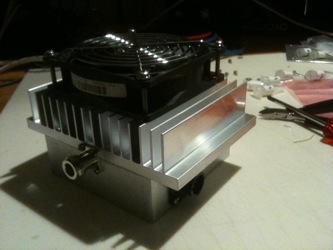
Interesting ? Yes but... before thinking to use this kind of gizmo after the USRP, the RF signal need some manipulations, avoiding any disturbance on the radio spectrum.
- Update 24/2/2010: Check the new WBX daughterboard test, a big improvement for a clean spectrum !
NEVER CONNECT TO AN ANTENNA WITHOUT A LICENSE !
Output Spectrum
Usually when somebody need to transmit easily voices information on the radio spectrum he use an oscillator directly modulated and tuned on the working frequency. To avoid unwanted signals outside the working band (harmonics) low pass filters are mainly used after this oscillator and amplifiers.
It is also possible to use RF mixer to up convert the frequency from the modulated oscillator on a higher band when intermediate line is used to carry the RF signal from the modulator stage to the up-converter / power amplifier. (This is mainly used on Terrestrial link, Uplink Earth Station, Vsat terminals and help to avoid to much losses when you carry a very high frequency signal) This allow also frequency agility on a larger band. In this case a mix of high pass and low pass or bandpass filters are used to keep the energy where it should be !
USRP boards propose different band coverage and use direct output from the DA's or converted RF spectrum. As we use digital modulation (OFDM in this case... including amplitude modulation) we need a good linearity on the RF chain path to avoid distortion added to the source signal. Amplifiers will not work near their saturation point but where we get the best linearity. (I & Q frame are send from the PC to the USRP FPGA, after computing, signal is applied to DA's to generate the modulation in the 'analog world'. In the case of RF mixing for band conversion we should also ensure that we do not introduce too much phase noise (mainly from the up-converter local oscillator)
USRP BasicTX
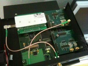
Test with the BasicTX: On the picture you see the board installed inside the USRP, TX A port (Upper right) This board take the signal from the DA's and provide the output with SMA connectors via a transformer. The don't use any actives components, you get after the transformer what you have directly from the DA. When we generate a signal on this board we have measured a total power of 18 uW. (with 50 ohm load 0 dB of gain in the gnuradio module)
As we use one DA from the TX A port (USRP have two DA's with balanced output on each port) we get a real signal at the output, meaning that you get every harmonics and image frequency till they go in the noise floor (bandwidth of the onboard transformer used to unbalance and adapt the output inpedance)
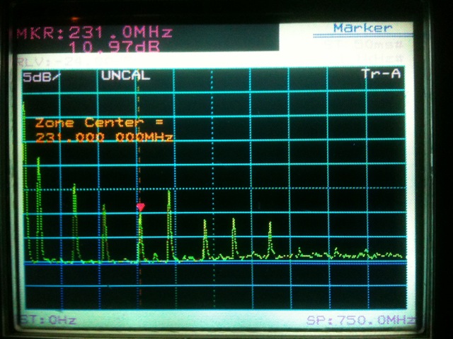
This is typically how looks the output spectrum of the BasicTX.
Note the red marker showing the desired working frequency in the Band III (see Band 3 Channels) (exact value: 12C @227.360 Mhz during the measurement).
To filter the lower and stronger peaks will required more than 80 dB of attenuation and the same for the next upper peak ! The picture show the spectrum from 0 to 750 Mhz
So ! this will required further filtering before applying any pre amplifier stage...
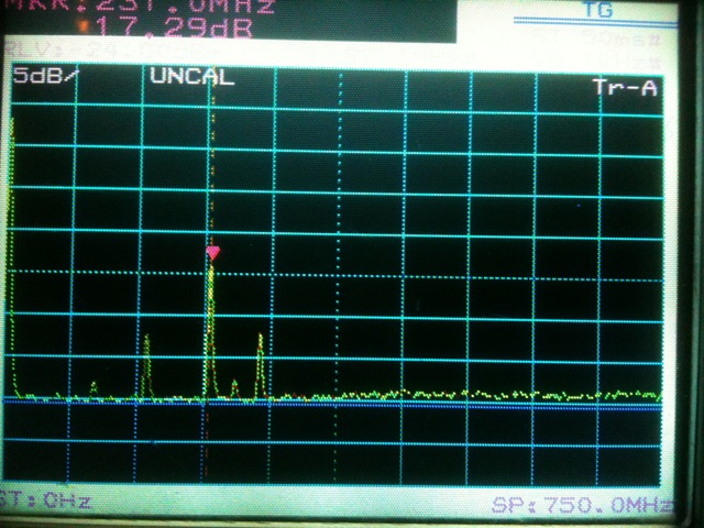
The same now but with a first filtering trial... we still have to much unwanted carriers near the working band !!! TBC...
USRP RFX400
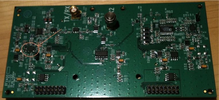
The RFX400 can work from 400Mhz to 500 Mhz with a total power up to 200 mW. To use it for the band III on the channels 10,11,12 we need to make some modification.
The conversion is done with a quadrature modulator (AD8345) taking the two DAC's USRP TX port signal and a carrier from a built in programmable local oscillator (PLL using one ADF4360). The card include also for the TX path 2 stages of amplification before a low pass filter. The bandwidth of the last stage will not go under 300 Mhz (According to the spec. of the RF3315 rated for 0.3 to 3 Ghz).
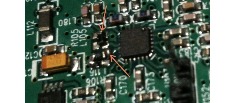
If you try to use this card under 400 Mhz you need at least to change the inductances value of the PLL vco. (He won't lock outside the original band) According to the chip data-sheet the correct value to go on the band III is around 22 nH.
Locate the TX PLL:
Then replace L105 and L115 inductances (in // with R105 and R106)
(Note: Since the RFX400 use the same PLL design beetween RX and TX side, this could be done at the RX path, if you want to receive signal on the same band, just replace L31 & L32 as done at the TX side)
We had no problem after this modification to lock beetween 200 to 235 Mhz. (Note: When having RFX400 and BasicTx installed simultaneously inside the USRP the software will adress by default the BasicTX !)
Whithout changing the amplifier (remember, we are bellow 300 Mhz the lower limit of the last stage) we still have an average of 5 mW at the output.
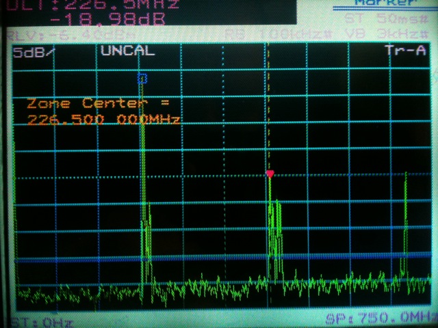
As for the BasicTX this is how look the output spectrum of the RFX400:
We see that working below the original board band will require to change the value of the on-board lowpass filter in order to kill the upper harmonics (that are now under the cutoff frequency of the filter, around 500MHz). The peak with the blue square is the wanted signal while the peak with the red marker is his first harmonic (in the original RFX400 band). The ratio between the in-band signal and the first harmonic is also degraded by the fact that we didn't change the final amplifier stage (RF2250 from RFMD, designed to operate from 300MHz to 3GHz), further improvements needs to be done...
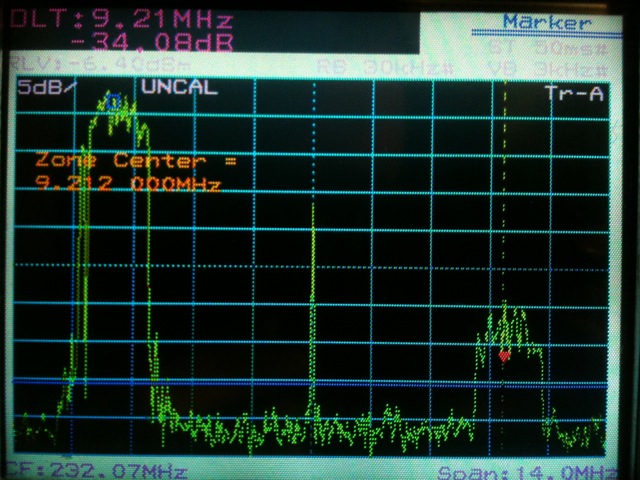
A closer look to the inband signal:
The LO leakage (center carrier on the picture) remain to high and require a strong attenuation before putting on the air this signal.
As the signal center frequency (modulated groupe of carriers from the OFDM signal) coming from the DAC's is quite low (4,7 Mhz) it keep the beat too close of the LO, making this hard to filter it efficiently without disturbing the linearity on the OFDM channel.
We also see that the upper beat signal (LO + 4,7 Mhz) is visible at 30 dB under the lower beat (LO – 4,7 Mhz = wanted signal). We should have a balance problem between the two inputs of the quadrature modulator (DC offset ? Averaging in the FPGA when computing the complex signal ? Resistors precision after the DAC's ?) This need to be investigated ...
As different elements of this spectrum are not so easy to filter (very close in frequency) it might be wise to change the center frequency leaving the DAC's (limited by the sampling rate) to make a wider space and use a higher LO frequency. This to put a fixed mask filter after the DAC's, then low pass filters after the quadrature modulator to kill the LO, the upper beat signal (if we cannot balance perfectly the input source at the modulator) and higher harmonics. Then we will replace the final stage of the RFX400 board by a monolytic amplifier having a lower 'start frequency'.
Update: For the RFX400 the command to change the offset between the LO from the PLL and the DAC's signal at the input of the quadrature modulator is: device.set_lo_offset(freq in Hz)
For example to get an offset of 44 Mhz: device.set_lo_offset(44000000)
USRP with WBX daughterboard
Check the new WBX daughterboard test, a big improvement for a clean spectrum ! (Update 24/2/2010)
Filters
Filtering will be crucial to get something that we can put on the air without jamming anybody else... Before doing a specific design we have first tested different USRP boards to get a clearer view of what we should do to achieve a good result. We will go into details after having tested a fully modified RFX400 or building our own up-converter board.
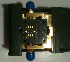
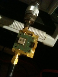
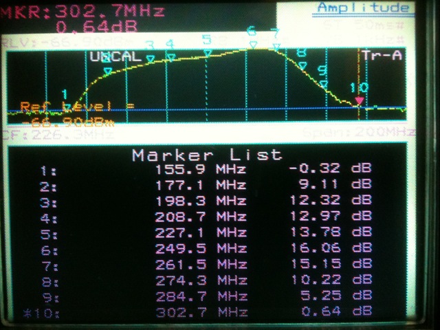
Nevertheless some evaluation with easy solution (before going to design dedicated boards) show some good examples, 3 bandpass filters from Mini-circuit where used to evaluate linearity between our concatenated power stage... and it give good hopes !
Evaluation board for one filter cell:
The filter under test (RBP-220W)
Characteristic of one bandpass cell loaded at 50 ohm (in & out)
TBC...
Power Stage
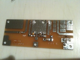
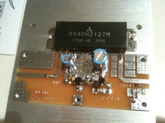
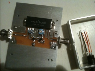
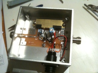
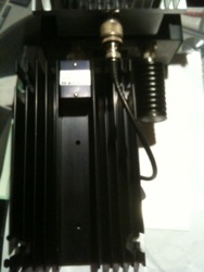
Power Amplifier cooling modification / input strip line filter mod / padding / Current Bias adj for better linearity / gain - input power TBC...
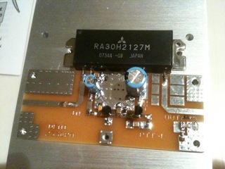
This amplifier use a 30 Watt Mosfet Module from Mitsubishi:
http://www.mitsubishichips.com/China/common/cfm/ePartProfile.cfm?FILENAME=ra30h2127m.pdf
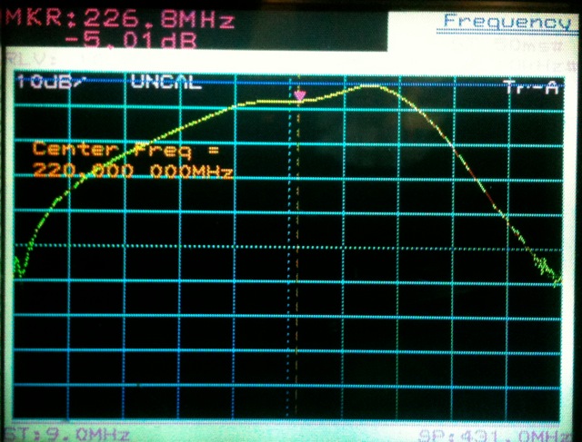
The measured gain at 220 Mhz on the one in stock here is 36 dB.
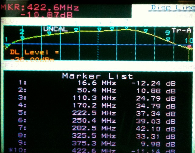
With a small signal at the input (1 mW) we get the following gain response when sweeping the signal from 6 to 450 MHz (without any filter)
The second photo give more detail on the characteristic, the blue line is the power level at the input of the amplifer, the value in dB are relative to the input power.
When driving this module with the OFDM signal from the USRP we keep a linear signal until 15W, 16W maximum at 220 MHz, higher will add distortion on the signal, maybe pre-corection at the modulation could allow us to get a little bit more from it.
Using the WBX daughterboard followed by a one filter cell from Minicircuit for band 3 we obtain for g (in the Dwap player command line):
| DWAP Gain (-g x) | Power Output |
|---|---|
| 2 | 80 mW |
| 3 | 150 mW |
| 4 | 225 mW |
| 5 | 400 mW |
| 6 | 700 mW |
| 7 | 1.2 W |
| 8 | 1.6 W |
| 10 | 3.2 W |
| 11 | 4.5 W |
| 12 | 6 W |
| 13 | 7.8 W |
| 14 | 10 W |
| 15 | 13 W |
Setup Pictures
Just for fun and to show that it is really working ;) A short video here !
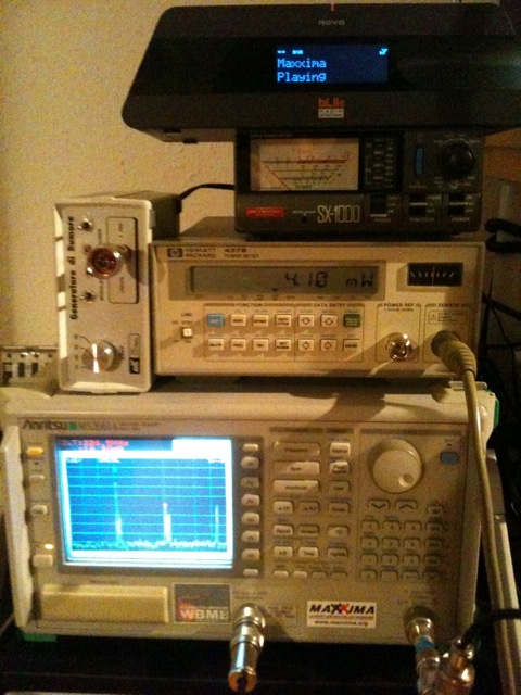
First everything on dummy load ! (especialy when you rize more than a few uW... )
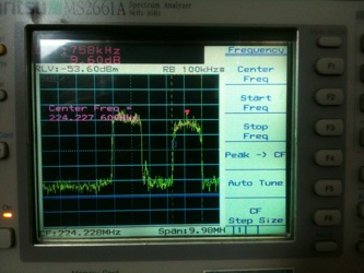
... and the measurement setup.
The left carrier is the swiss public mux services @Channel 12A and on the 12C our carrier.
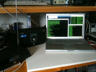
The PC receiving 5 Internet streams or live sounds from onboard PC audio card, re-encoding, muxing, modulating I & Q frame sending it to the USRP via USB...
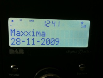
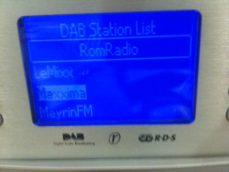
One receiver...
Another one when selecting audio programs on the mux...
If you want to know every aspect involved in digital audio broadcasting you must have this book ! Mister MC borrow one to me and it's a must have ! (we have nothing to do with Wiley publication or the authors, I just found it very useful !)
